GeoComp benchmarks
Research Group on Geo-Information Computing (GeoComp)
Solder Paste Scooping Detection by Multi-Level Visual Inspection of Printed Circuit Boards
by Csaba Benedek, Olivér Krammer, Mihály Janóczki and László Jakab
Published in IEEE Trans. on Industrial Electronics (access the paper in IEEE Xplore) [1]
Abstract
In this work we have introduced an automated Bayesian visual inspection framework for Printed Circuit Board (PCB) assemblies, which is able to simultaneously deal with various shaped Circuit Elements (CE) on multiple scales. We have proposed a novel Hierarchical Multi Marked Point Process (HMMPP) model for this purpose, and demonstrated its efficiency on the task of solder paste scooping detection and scoop area estimation, which are important factors regarding the strength of the joints. A global optimization process attempts to find the optimal configuration of circuit entities, considering the observed image data, prior knowledge, and interactions between the neighboring CEs. The computational requirements are kept tractable by a data driven stochastic entity generation scheme. The proposed method is evaluated on real PCB data sets containing 125 images with more than 10.000 splice entities.Results were partially introduced in Pattern Recognition Letters [2] and also presented in the ICIP 2011 [3] conference.
Introduction
Defect detection by Automatic Optical Inspection (AOI) is a crucial step during the manufacturing process of Printed Circuit Boards (PCB). Recent developments in resolution, quality and speed of the industrial cameras have opened several new prospects and challenges in image based verification. This improvement enables the investigation of several previously unrecognizable features and artifacts, which can effect various phases of the manufacturing process. PCB inspection is a strongly inter-disciplinary task, as it encapsulates problems raised by industrial technology (estimating the effects of the artifacts), optics (exploiting up-to-date imaging devices, and dealing with their limitations) and advanced vision based quality assessment and pattern recognition approaches .
In this work we have proposed a hierarchical visual inspection framework, which implements a multi-level entity extraction approach. We introduced this model suited to a selected AOI task, called scooping detection, since scooping is a significant practical problem influencing the strength of solder joints in stencil prints. On the other hand, the relationship between the solder joints and the embedded scoops can be described by a clear hierarchical structure, thus the methodology of the proposed approach may be adopted to various AOI tasks.
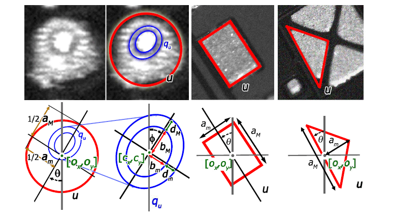
The input of the proposed method is an optical image taken from a PCB with printed Solder Pastes (SP). The goal is to detect and separate the SPs, and simultaneously extract the scoop artifacts, which may appear in some pastes. We approximate the shape of the SPs by various plane figures from a shape library, in this paper ellipses, rectangles and isosceles triangles are used. On the other hand, we model a Scoop Object (SO) by two concentric ellipses as it consists of a bright central region (inside the internal ellipse) and a relatively darker elliptical ring (region between the internal and external ellipses) enclosed by the brighter SP patch Fig. 1.
Outline of methodologyical contribution
Marked Point Processes (MPP) provide efficient tools to extend conventional Markov Random Field (MRF) based pixel level classification techniques, by taking into account the geometry in the proposed models. An MPP model works with objects as variables rather than with pixels, so that the number of variables is also unknown. However, implementing a multi-level PCB inspection task is challenging in the MPP framework:
- Hierarchy: PCB elements appear at multiple hierarchical levels, e.g. Solder Pastes (SPs) and included scoops.
- Heterogeneity: SPs have various geometric shapes.
- Multi-scaling: SP sizes are in different orders of magnitudes.
For these reasons, we introduce here an new Hierarchical Multi Marked Point Process (HMMPP) model with the following three key properties:
We describe the hierarchy between objects and object parts as a parent-child relationship embedded into the MPP framework.
To simultaneously deal with variously shaped circuit elements, we jointly sample different types of geometric objects, by adopting the multi-marked point process schema to the hierarchical entity extraction problem.
To efficiently sample the SP population space, we develop a Bottom-Up (BU) stochastic object proposal strategy, by combining low level statistical image descriptors with prior information based structure estimation. This step keeps the computational complexity tractable, although due to the above two properties the dimension and size of the solution space are significantly increased.
Entity models and feature extraction
The input of the proposed method is an optical image taken from a PCB with printed Solder Pastes (SP). The goal is to detect and separate the SPs, and simultaneously extract the scoop artifacts, which may appear in some pastes. We approximate the shape of the SPs by various plane figures from a shape library, in this paper ellipses, rectangles and isosceles triangles are used. On the other hand, we model a Scoop Object (SO) by two concentric ellipses as it consists of a bright central region (inside the internal ellipse) and a relatively darker elliptical ring (region between the internal and external ellipses) enclosed by the brighter SP patch Fig. 1.
Fig. 1. Notations of the diffetent geometric models of a Solder Joint (u) and the bi-elliptical scooping effect (q)
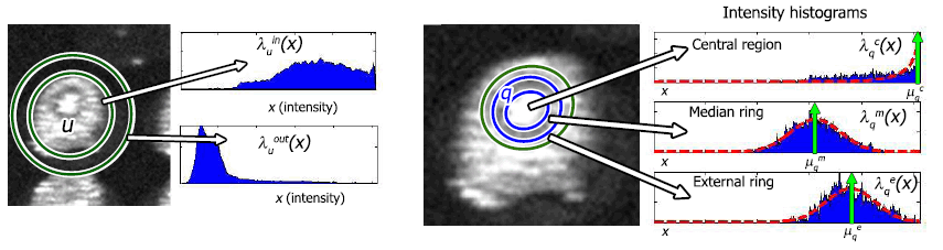
In the obtained circuit images the parent Solder Pastes appear as bright patches surrounded by darker background. To evaluate the contrast between the SPs and the board, we calculate the Bhattacharya distance between the pixel intensity distributions of the internal SP regions and their boundaries. As for the scoop modeling, we distinguish three regions of each scoop: the central bright ellipse, the darker median ring and the bright external ring. Data based Features are demonstrated in Fig. 2.
Fig. 2. Data based features regarding SP (left) and Scoop (right) modeling.
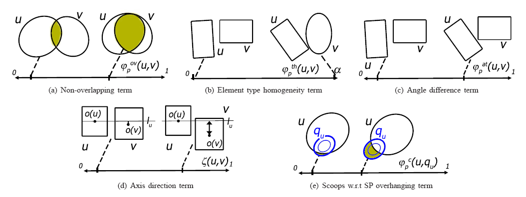
We also use different interaction terms which evaluate a given configuration on the basis of prior geometric constraints (see Fig. 3). Since we aim to extract individual SP entities, we must penalize overlapping between different SP objects. In PCBs we can often observe that several SPs with the same type form spatially connected groups. Relying on this prior assumption, we should favor SP configurations, where the neighboring entities have mostly identical types which can be expressed by the Potts constraint. Finally, SPs in the printed boards are usually aligned, i.e. most of the neighboring entity pairs are either parallel or perpendicular. While previous prior terms prescribe soft constraints between SP objects, we define the Encapsulation condition between a given SP and its included scoop. Here we penalize if a scoop overhangs its parent paste, which is measured by the overhanging area normalized by the area of the scoop.
Fig. 3. Prior terms in the model
Optimization
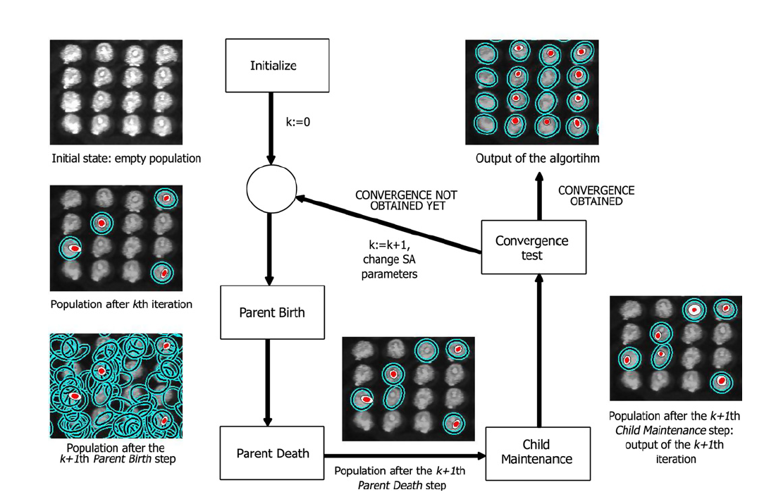
Due to time and quality constraints of the manufacturing process, the computational efficiency and detection performance of the optimization plays a particularly crucial role in the addressed application. We can find an extensive bibliography for MPP energy minimization. However, in most of the rpevious models, the dimension and extension of the object parameter space is relatively small. Conversely, the proposed HMMPP model must deal with variously shaped and scaled circuit elements, while the embedded SOs increase onwards the dimension of the object descriptor vector. As a comprise, we supplement the Multiple Birth and Death (MBD) algorithm with three simple moves: shape perturbation, type change and child maintenance, so that the optimization in the multidimensional parameter space is decomposed to computationally efficient steps. On the other hand, instead of applying fully random sampling, we construct a data driven stochastic entity generation scheme, which proposes relevant SPs with higher probability based on various image features. The main steps of the hierarchical MBD optimization can be followed in Fig. 4.
Fig. 4. Optimization: Hierarchical Multiple Birth and Death Algorithm
Experiments
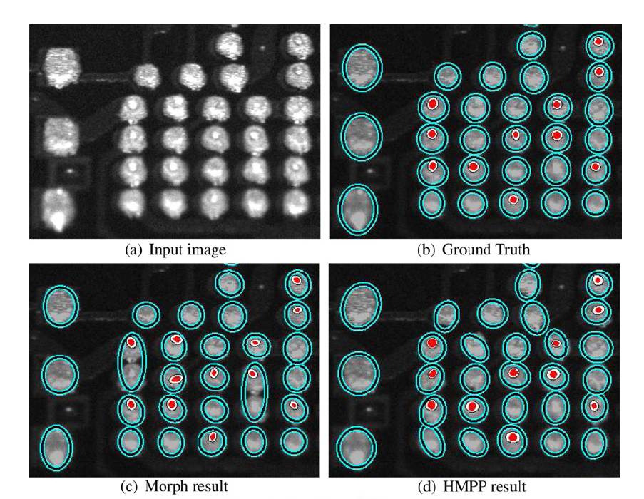
We have tested the proposed model on a three real PCB datasets: SetHeavy contains 44 images with heavy scooping ratio of 14% (664 scoops in 4655 SPs), while SetSparse includes similar PCB photos, with a much lower SO rate of 3% (112 scoops out of 4100 pastes in 66 images). In the third collection, SetDark (1283 pastes in 12 images), the scooping artifact does not appear at all, however, due to lower image quality the accurate SP extraction step is more challenging. The circuits contain variously shaped Solder Pastes, in particularly elliptical, rectangular and triangular elements. Some qualtitative results, compared to a baseline technique, called Morph are shown in Fig. 5 and 6. For detailed evaluation results (including various quantitative parameters), please check the corresponding publications.
Fig. 5. Qualitative evaluation: the proposed HMMPP model comared to the baseline Morph technique
Fig. 6. Evaluation on a sample with different SP shapes
References
[1] Cs. Benedek, O. Krammer, M. Janóczki and L. Jakab: ”Solder Paste Scooping Detection by Multi-Level Visual Inspection of Printed Circuit Boards”, IEEE Trans. on Industrial Electronics , vol. 60, no. 6, pp. 2318 - 2331, 2013
[2] Cs. Benedek, ”Detection of Soldering Defects in Printed Circuit Boards with Hierarchical Marked Point Processes,” Pattern Recognition Letters, vol. 32, no. 13, pp. 1535-1543, 2011
[3] Cs. Benedek: ”Analysis of Solder Paste Scooping with Hierarchical Point Processes,” IEEE International Conference on Image Processing (ICIP), Brussels, Belgium, September 11-14, 2011

Links
Geo-Information Computing @ Machine Perception Lab.
GeoComp Demos:
Contact
GeoComp Group leader: Prof. Csaba Benedek benedek.csaba@sztaki.hu
i4D project manager: Dr. Zsolt Jankó janko.zsolt@sztaki.hu
Head of MPLab: Prof. Tamás Szirányi
MPLab administration: Anikó Vágvölgyi
Address:
SZTAKIKende utca 13-17
H-1111 Budapest, Hungary Tel: +36 1 279 6097